| Sign In | Join Free | My autoplansearch.com |
|
- Home
- Products
- About Us
- Quality Control
- Contact Us
- Get Quotations
| Sign In | Join Free | My autoplansearch.com |
|
Brand Name : xingqiang
Model Number : Varies by goods condition
Certification : ROHS, CE
Place of Origin : China
MOQ : Sample,1 pc(5 square meters)
Price : NA
Payment Terms : ,T/T,Western Union
Supply Ability : 100000㎡/Month
Delivery Time : 12-15 work days
Product : Print Circuit Board
Max.Board Size : 528*600mm
Minimum Line Space : 3mil (0.075mm)
Surface Finishing : HASL/OSP/ENIG
Material : FR4
Pcba Standard : IPC-A-610 E Class II-III
Production : Gerber Files or BOM List
Board Thinkness : 1.6/1.2/1.0/0.8 or Customized
Layer Counts : 2/4/6/8/10L or Customizable
Ink Color : Green/Red/Yellow/White/Black/Blue
FR4 OSP Surface Finishing Process
A Multilayer Printed Circuit Board (PCB) is a sophisticated assembly consisting of three or more conductive copper layers laminated together under high pressure and heat, with insulating materials (such as core and prepreg) separating each layer. Unlike single-sided boards, this complex structure enables high-density wiring and superior signal integrity.
Main Advantages of Multilayer PCB:
| 1. Enhanced Signal Integrity | • Separates signal layers from power/ground layers, reducing crosstalk between adjacent signal traces. • Provides a dedicated reference plane (ground or power) for signal layers, minimizing signal reflection and transmission loss. |
| 2. Higher Component Density & Space Savings | • Allows routing of traces on four layers instead of two, enabling more complex circuit designs in a smaller board area. • Reduces the need for through-hole vias or jumper wires, making the board layout more compact and suitable for miniaturized devices. |
| 3. Improved Electromagnetic Compatibility (EMC) | • Dedicated power and ground layers form a stable "power-ground plane capacitor," filtering out high-frequency noise. • Isolates sensitive analog signals from noisy digital circuits by placing them on separate layers, reducing electromagnetic interference (EMI) emissions and susceptibility. |
| 4. Cost-Effectiveness for Complex Designs | • More economical than 6-layer or higher-layer PCBs when basic 2-layer boards cannot meet performance requirements. • Lowers overall system costs by reducing the need for additional external components (e.g., noise filters) that compensate for poor signal or EMC performance. |
How to order multi-layer boards?
Send us your customizable Files:
1. Gerber files (RS-274X)
2. BOM (if PCBA needed)
3. Impedance requirements & stack-up (if available)
4.Test requirements (TDR, network analyzer, etc.)
Tip:Normally,Gerber files includes: PCB type,thickness, ink color, surface treatment process, and if SMT processing is required, you can provide a component BOM and reference designation diagram, etc.
We’ll reply within 24 hours with a free quote, DFM report, and material recommendation.

Factory showcase

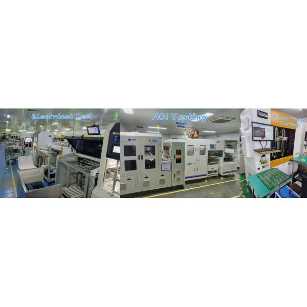
PCB Quality Testing

Certificates and Honors


|
|
FR4 OSP Surface Multilayer Printed Circuit Board 4 Layer PCB Board OEM/ODM Service Images |